
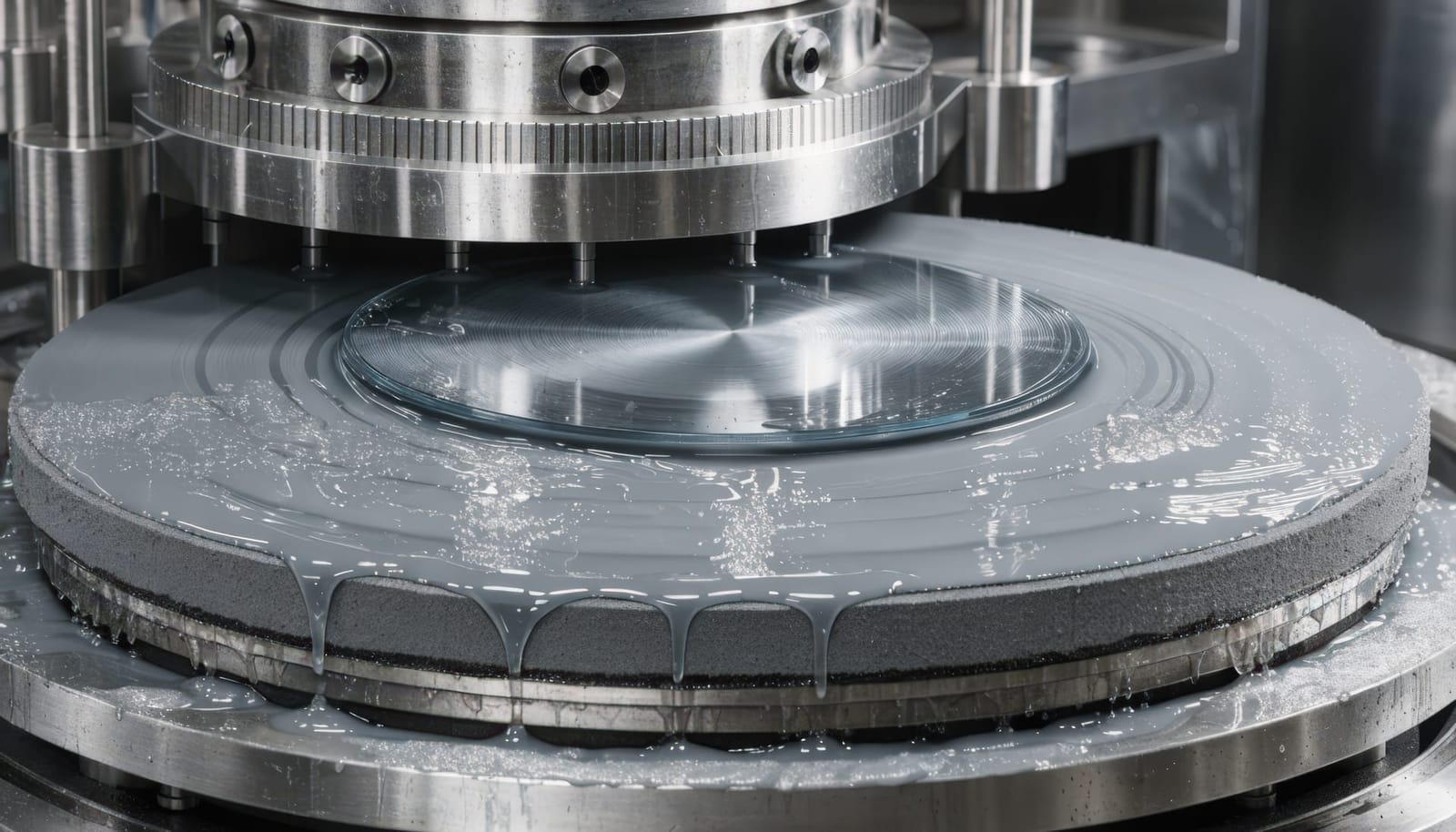
The other half of our Hillsboro production: ceria-based CMP slurries for chemical mechanical planarization. AGC is fully integrated from abrasive particle synthesis through finished slurry, and AGCEA brings that integrated production to the US. Controlling every variable from ceria synthesis up through chemical formulation lets us tune custom recipes for process-specific applications, hold lot-to-lot consistency tighter than blended-ingredient suppliers, and respond to fab-specific qualification work without sourcing-chain handoffs.
The flagship product lines are CES-300 series (for shallow trench isolation, STI applications) and CES-330F series (for interlayer dielectric, ILD applications), both formulated in Hillsboro, Oregon.
What sets the formulation apart
CMP requires the simultaneous chemical and mechanical removal of material at rates that differ predictably across the films on a wafer. The challenge is selectivity (how aggressively the slurry attacks one film relative to another) and uniformity, both within a wafer and from wafer to wafer.
The CES series is engineered for:
- High step-flattening. Planarization efficiency across the topography of patterned wafers.
- Material selectivity. Tunable removal-rate ratios between SiO₂, SiN, poly-Si, metals, and resins.
- Removal rate control. Predictable polish rates from front-end oxide CMP through back-end interconnect work.
- Uniformity. Within-wafer and wafer-to-wafer consistency that meets the requirements of leading-edge fabs.
- Low defectivity. Reduced count of scratches, pits, and residual abrasive.
- US-based formulation. Manufactured at our Hillsboro, Oregon site for the North American domestic supply chain and for global semiconductor customers.
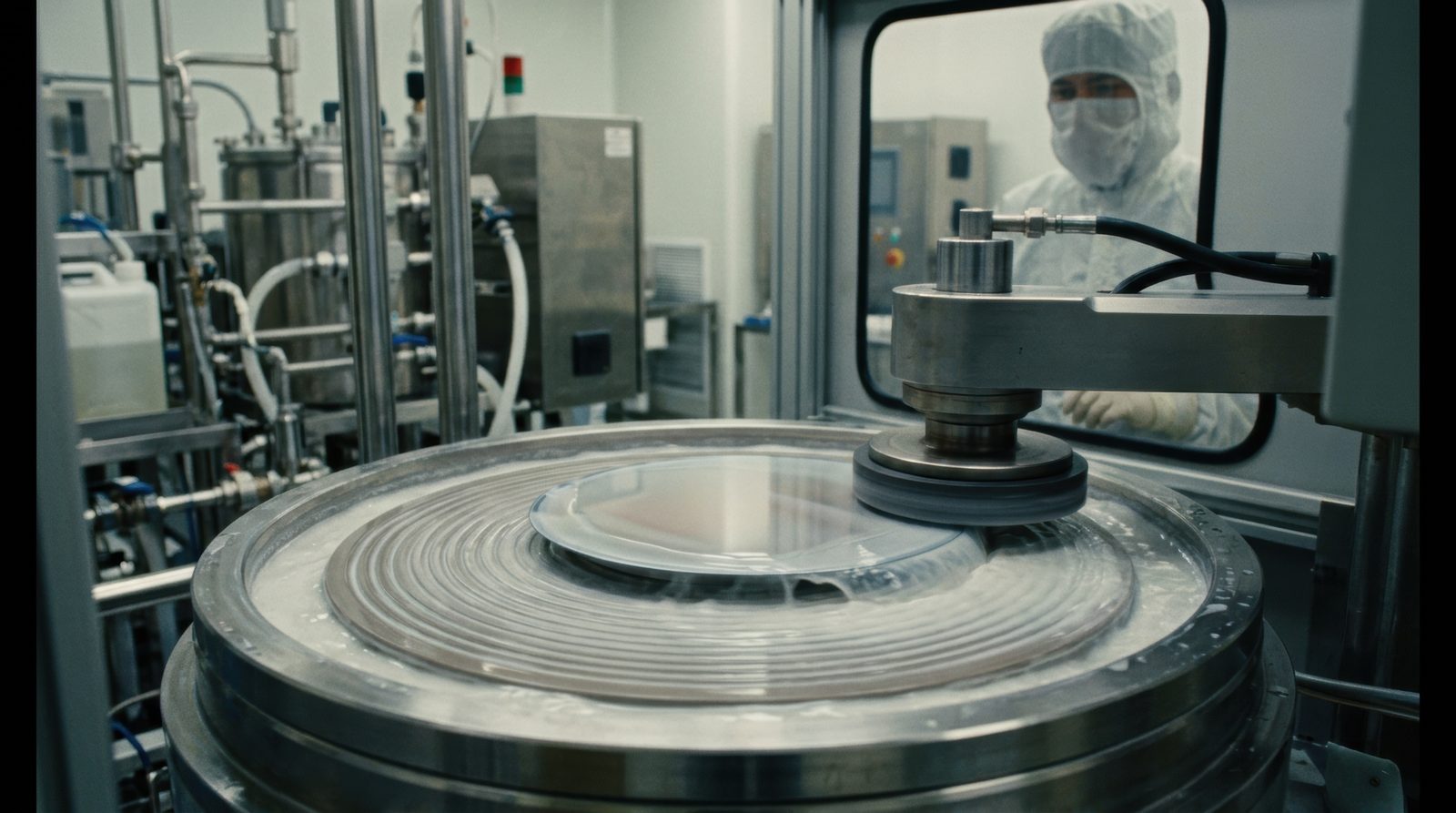
Chemical-mechanical planarization in action: a wafer polished against a rotating, slurry-flooded platen under the polishing head, monitored from the cleanroom.
Two-component and one-component supply
The CES series supports both one-liquid and two-liquid supply methods, allowing customers to choose the format that best fits their existing wet-bench infrastructure and process recipe.
Technical support
Our Hillsboro team works directly with US semiconductor customers on slurry selection, process integration, and ongoing performance qualification. For new applications, we co-develop recipe windows with the fab and tune particle size, chemistry, and dilution to the production target.
Applications
- Front-end CMP: shallow-trench isolation (STI) and interlayer dielectric (ILD) planarization
- Back-end CMP: copper and tungsten interconnect polishing
- Advanced-packaging CMP: through-silicon via (TSV) and redistribution layer planarization
- Polishing of poly-Si, SiO₂, SiN, metals, and resin layers
Documents
- Spec Sheet (CES-300) Available on request
- Spec Sheet (CES-330F) Available on request
- Material Safety Data Sheet (MSDS) Available on request
- RoHS Declaration Available on request
- REACH Declaration Available on request
- ISO 9001:2015 Certificate Available on request
Specifications
Detailed specifications available on request. Use the form below.
Related materials
-
ROICERAM™-HS
Silicon Carbide
Silicon carbide ceramic components, recrystallized and CVD-coated, for vertical, horizontal, and single-wafer semiconductor furnace processes.
-
AQ Grade
Photomask Substrates
AQ-grade synthetic quartz substrates engineered for photomask manufacturing. Sub-100nm flatness per side and exceptionally low defect counts.